Objective: Develop and fabricate single and multilayer thin film diffractive and reflective optics, as well as experimental samples, primarily for APS beamlines and users. Staff are available for consultation regarding thin-film deposition materials selection, general optical component design, & simulation. The deposition laboratories include: 1) Class 10,000 clean room that houses a large DC sputtering system and a small deposition system; 2) Class 100, 000 clean room that house a rotary deposition system and a laboratory x-ray reflectrometer for evaluation of single and multilayer thin film optics; and 3) Class 10,000 class cleanroom that is used for beamline optical system mounting and for the development of the future APS mirror/multilayer modular deposition system. These laboratories are conveniently located near the Optics and Detector Testing beamline 1-BM, on the APS experiment hall floor. Work requests can be submitted by filling the Optics Group's work request from. | |
| (1.5 m) Sputter Deposition System | |
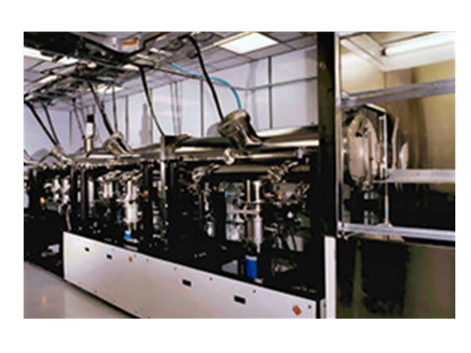
Our 1.5m deposition system accepts maximum substrate dimensions of 150 cm long, 20 cm wide, and 14 cm thick. Four sources combined with a broad-beam ion mill provide for a wide variety of mirror and sample coatings. | |
| Profile Coating System | |
| |
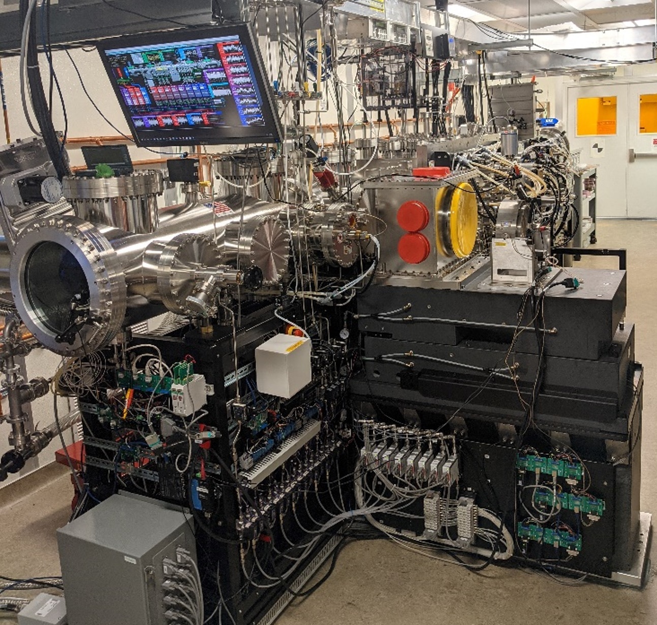
| Modular Deposition System | |
A precision multilayer and optics processing system equipped with multiple sources, the instrument is built with flexibility for new multilayer materials, techniques, instrumentation development, and in-situ diagnostics. Machine utilization includes multilayer and x-ray optical film deposition primarily for APS beamline applications. | |
| Thin Film Laboratory Capabilities | |
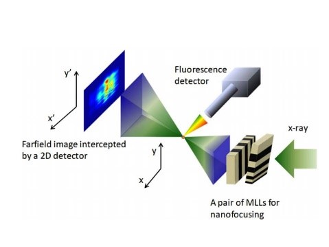
X-ray mirrors, multilayers and experimental samples are fabricated on a routine basis. Thousands of thin-film based optics and samples have been supplied to the APS user community over the history of the APS. We can reliably provide high-quality thin-film and multilayer optics and experiment samples, and we are constantly improving our equipment, techniques, and capabilities to satisfy the demand from the APS user community. In addition, we have the expertise to fabricate complete short focal length, fixed-geometry K-B mirror assemblies. | |
| Thin Film Research and Development | |
R&D in thin film optics is carried out jointly with the APS beamline scientists and user community, independently or in collaboration with other facilities to keep the group at the state-of-the art in x-ray optics. Examples include studies of new materials for mirrors, monochromators, and volume diffractive optics; thin film stress mitigation; thin film radiation damage; etc.
|


