The original NIST article can be read here.
Researchers from the National Institute of Standards and Technology (NIST) and Intel reported success using an x-ray scattering technique at the U.S. Department of Energy’s Advanced Photon Source, an Office of Science user facility, to accurately measure features on a silicon chip to within fractions of a nanometer, or about the width of a single silicon atom.
The achievement could make the experimental technology known as CDSAXS (critical-dimension small angle x-ray scattering) a top contender in the race to develop new in-line process control tools for measuring vanishingly small features on next-generation computer chips. The research was the subject of an article in the October 2015 Journal of Applied Crystallography.
“The semiconductor industry is running out of measurement methods that work non-destructively on their ever-smaller next-generation nanostructures,” said NIST materials scientist R. Joseph Kline, an author of the Journal of Applied Crystallography article. “These are by far the smallest and most complex shaped nanostructures characterized by CDSAXS. The results show that CDSAXS has the resolution to meet next-generation metrology requirements.”
With the size of lines, trenches, holes and other features on silicon slices shrinking to single-digit nanometers, measurement tools long used to monitor chip production are approaching their limits. Factor in the growing complexity of chip design—such as building stack-like transistors instead of flat ones, a shift begun with Intel’s introduction of FinFET transistors in 2011—and it’s easy to understand why semiconductor manufacturers are eager for improved measurement capabilities.
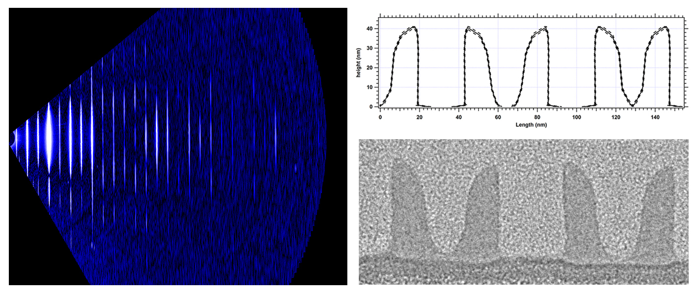
The NIST and Intel researchers used CDSAXS at the DuPont–Northwestern–Dow Collaborative Access Team 5-ID-D beamline at the Argonne APS to measure dimensions on silicon wafers fabricated at Intel’s research facilities with a periodic array of asymmetric lines. The array was made by pitch quartering, a method that quadruples the number of interconnect lines in a space that normally would accommodate only one. The intricate arrays of lines were made using multiple patterning steps chip makers now must employ to create features beyond the capabilities of existing light-based printing equipment. Throughout, getting precise measurements is critical; misalignments during the sequential patterning process can result in systematic errors, or flaws, in a chip.
A flaw of particular concern—and a focus of the NIST-Intel study—is pitch error, variations in the distance from one line edge to the next.
“The semiconductor industry has not only decreased product dimensions, but we’ve also developed increasingly complex 3D structures. These structures are becoming very difficult to characterize non-destructively with conventional in-line SEM [scanning electron microscope],” said Scott List, principal engineer in Intel’s Components Research Group. “Early results of NIST’s state-of-the-art CDSAXS measurements of these nanometer-sized structures have provided very useful atomic scale resolution of their 3D profiles.”
In the custom-made sample scrutinized in the study, lines resembling shark fins were 12 nanometers wide. The space between lines varied ever so slightly—by less than 0.5 nanometer—from a pitch of 32 nanometers.
CDSAXS measurements of periodic pitch errors—deviations from 32 nanometers—were accurate to within 0.1 nanometer; and measurements of line shapes were accurate to about 0.2 nanometer.
Since 2000, NIST has been pioneering the application of small-angle x-ray scattering to meet the ever-more demanding measurement needs of the semiconductor industry, which, for decades, has been doubling the density of transistors on a chip about every two years in accordance with Moore’s Law. Today’s leading-edge integrated circuits squeeze several billion transistors on a slice of silicon smaller than a typical postage stamp.
Currently used dimensional metrology tools rely on visible and ultraviolet light with wavelengths much larger than the features being measured. The x-rays used in CDSAXS have a wavelength less than 0.1 nanometer, much smaller than the dimensions of features on future generations of computer chips. CDSAXS exploits the short wavelength of x-rays and their sensitivity to differing densities of electrons in the materials they strike.
The noncontact, non-destructive technique does not require any sample preparation, and it works with test structures already used by semiconductor makers. CDSAXS, however, does not yield the equivalent of an x-ray picture of, for example, a broken wrist. Rather, patterns of x-rays scattered by electrons in the nanostructure are captured by a detector, providing data to be crunched by computers to solve for the original shape.
The analyses compare the pattern of scattered x-rays to carefully developed shape models of arrays of nanostructured features on a surface. This data-fitting procedure may go through several million rounds before achieving a satisfactory match between simulated and measured patterns of electron densities.
Following other studies demonstrating the capabilities of CDSAXS for a host of nanoscale measurements, the NIST-Intel study on complex samples representative of next-generation semiconductor manufacturing shows that CDSAXS can deliver the desired dimensional resolution.
The results should provide further impetus for ongoing efforts to develop compact sources of x-rays with the intensity required for in-line CDSAXS in semiconductor manufacturing facilities.
See: D.F. Sunday1, S. List2, J.S. Chawla2, and R.J. Kline1*, “Determining the shape and periodicity of nanostructures using small-angle X-ray scattering,” J. Appl. Cryst. 48, 1355 (2015). DOI: 10.1107/S1600576715013369
Author affiliations: 1National Institute of Standards and Technology, 2Intel Corporation
Correspondence: *[email protected]
The DuPont-Northwestern-Dow Collaborative Access Team is supported by Northwestern University, E.I. DuPont de Nemours & Co., and The Dow Chemical Company. This research used resources of the Advanced Photon Source, a U.S. DOE Office of Science User Facility operated for the DOE Office of Science by Argonne National Laboratory under Contract No. DE-AC02-06CH11357.
Argonne National Laboratory is supported by the Office of Science of the U.S. Department of Energy. The Office of Science is the single largest supporter of basic research in the physical sciences in the United States, and is working to address some of the most pressing challenges of our time. For more information, please visit science.energy.gov.

