The original CNRS press release can be read here.
In the race towards miniaturization, a French-U.S. team of researchers from the CNRS, Université de Lille, Université de Nantes as part of the Research Network on Electrochemical Energy Storage (RS2E) and Argonne National Laboratory has succeeded in improving the energy density of a rechargeable battery without increasing its size (limited to a few square millimeters in mobile sensors). This feat was achieved by developing a three-dimensional (3-D) structure made of microtubes, the first step towards producing a complete microbattery. The first experiments, including studies at the U.S. Department of Energy’s Advanced Photon Source (APS) have demonstrated the excellent conductivity of the battery's solid electrolyte, whose highly encouraging performance is published in the journal Advanced Energy Materials.
In the era of connected devices, intelligent connected microsensors require miniature embedded energy sources with great energy density. For ultra-thin—or planar—microbatteries, increased energy density means using thicker layers of materials, which has obvious limitations. A second method—used by the authors of the publication—consists in machining a silicon wafer and producing an original 3-D structure made of simple or double microtubes. 3-D batteries keep their 1 mm2 footprint area, but develop a specific area of 50 mm2—an enhancement factor of 50! These robust microtubes are large enough (of the order of the micron) to be coated with multiple layers of functional materials.
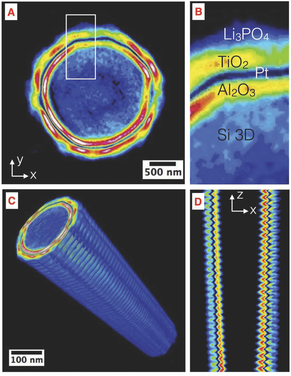
The main technological challenge consisted precisely in depositing the different materials that make up the rechargeable battery in thin and regular layers on these complex 3-D structures. Using the cutting edge technology of Atomic Layer Deposition (ALD), the materials perfectly took on the 3-D shape of the template without blocking the tube structures. In this way the researchers created an insulating thin film, a current collector, a negative electrode, and a solid electrolyte. The various analyses and characterizations, including synchrotron x-ray nanotomography at the X-ray Science Division 32-ID x-ray beamline at the Argonne APS (an Office of Science user facility) and transmission electron microscopy show that the successive layers are of excellent quality, showing conformality of nearly 100%. The interfaces are clean (no interdiffusion between the different chemical elements), with no pinholes, cracks, or fissures detected.
Lithium phosphate, the electrolyte of this future 3-D microbattery, is in solid form. After depositing it using the same ALD technology, researchers showed that it has a high electrochemical stability window (4.2 V), high ionic conductivity, and low thickness (10 to 50 nm), which generates low surface resistance, all of which are very encouraging for the future performance of the 3-D battery.
The next step will consist in using ALD to develop thin films of positive electrode materials in order to create the first functional 3-D prototypes, which will certainly offer much greater performance than today's planar microbatteries.
See: Manon Létiche1,2,3, Etienne Eustache1,3,4, Jeremy Freixas1,3,4, Arnaud Demortière3,5, Vincent De Andrade6, Laurence Morgenroth1, Pascal Tilmant1, François Vaurette1, David Troadec1, Pascal Roussel2, Thierry Brousse3,4, and Christophe Lethien1,3*, “Atomic Layer Deposition of Functional Layers for on Chip 3D Li-Ion All Solid State Microbattery,” Adv. Energy Mater., 1601402 (2016). DOI: 10.1002/aenm.201601402
Author affiliations: 1Université de Lille Sciences et Technologies, 2Université Lille 1 Sciences et Technologies, 3Réseau sur le Stockage Electrochimique de l’Energie, 4Université de Nantes, 5Université de Picardie Jules Verne, 6Argonne National Laboratory
Correspondence: *[email protected]
This research was financially supported by the ANR and the DGA within the MECANANO project (ANR-12-ASTR-0032-01). The authors also want to thank the French network on the electrochemical energy storage (RS2E), the Store-Ex Labex, the French RENATECH network for the financial support. C. Brillard from IEMN is also thanked for the AFM top surface analysis. Finally, the Fonds Européen de Développement Régional (FEDER), CNRS, Région Nord Pas-de-Calais, and Ministère de l’Education Nationale de l’Enseignement Supérieur et de la Recherche are acknowledged for funding. This research used resources of the Advanced Photon Source, a U.S. Department of Energy (DOE) Office of Science User Facility operated for the DOE Office of Science by Argonne National Laboratory under contract no. DE-AC02-06CH11357. This work is patented: "Substrat microstructuré," C. Lethien, P. Tilmant, E. Eustache, N. Rolland, T. Brousse, WO2015/052412 A1.
Argonne National Laboratory seeks solutions to pressing national problems in science and technology. The nation's first national laboratory, Argonne conducts leading-edge basic and applied scientific research in virtually every scientific discipline. Argonne researchers work closely with researchers from hundreds of companies, universities, and federal, state and municipal agencies to help them solve their specific problems, advance America's scientific leadership and prepare the nation for a better future. With employees from more than 60 nations, Argonne is managed by UChicago Argonne, LLC for the U.S. Department of Energy's Office of Science.
The U.S. Department of Energy's Office of Science is the single largest supporter of basic research in the physical sciences in the United States and is working to address some of the most pressing challenges of our time. For more information, visit the Office of Science website.

