The original Washington State University press release can be read here.
The long-standing scientific challenge of watching a material change its crystal structure in real time has been met by Washington State University (WSU) researchers using high-brightness x-ray beams and dynamic compression experiments at the U.S. Department of Energy’s Advanced Photon Source (APS).
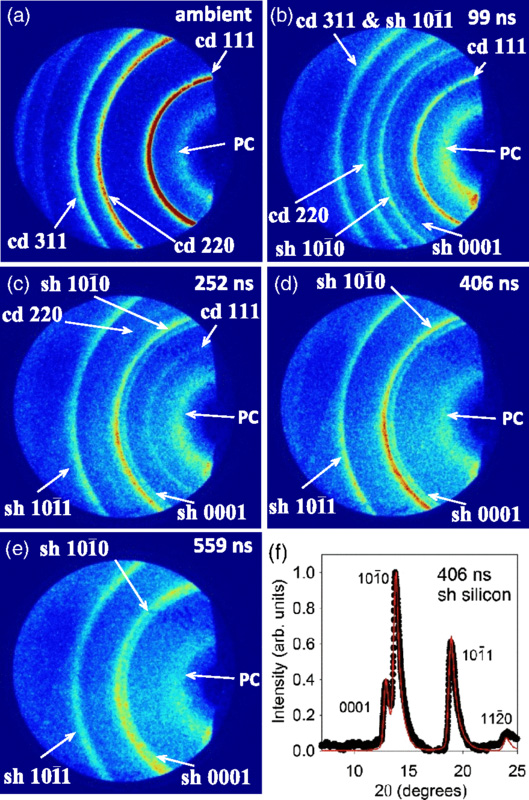
While exposing a sample of silicon to intense pressure—due to the impact of a nearly 12,000-mph plastic projectile—the researchers documented the transformation from the silicon’s common cubic diamond structure to a simple hexagonal structure. At one point, they could see both structures as the shock wave traveled through the sample in less than half a millionth of a second.
Their discovery is a dramatic proof of concept for a new way of discerning the makeups of various materials, from impacted meteors to body armor to iron in the center of the Earth.
Until now, researchers have had to rely on computer simulations to follow the atomic-level changes of a structural transformation under pressure, said Yogendra Gupta, Regents professor and director of the WSU Institute of Shock Physics. The new method provides a way to actually measure the physical changes and to see if the simulations are valid.
"For the first time, we can determine the structure," Gupta said. "We've been assuming some things but we had never measured it."
Writing in Physical Review Letters, the researchers say their findings already suggest that several long-standing assumptions about the pathways of silicon's transformation "need to be reexamined."
The discovery was made possible by a new facility, the Dynamic Compression Sector (DCS) at the APS, an Office of Science user facility located at Argonne National Laboratory. Designed and developed by WSU in partnership with the APS, the DCS is sponsored by the U.S. Department of Energy's National Nuclear Security Administration, whose national security research mission includes fundamental dynamic compression science. The APS provided high-brilliance x-ray beams that pass through the test material and create diffraction patterns that the researchers use to decode a crystal changing its structure in as little as five billionths of a second.
"We're making movies," said Gupta. "We're watching them in real time. We're making nanosecond movies."
Stefan Turneaure, lead author of the Physical Review Letters paper and a senior scientist at the WSU Institute for Shock Physics, said the researchers exposed silicon to 19 gigapascals, nearly 200,000 times atmospheric pressure. The researchers accomplished this by firing a half-inch plastic projectile into a thin piece of silicon on a Lexan backing. While x-rays hit the sample in pulses, a detector captured images of the diffracted rays every 153.4 nanoseconds—the equivalent of a camera shutter speed of a few millionths of a second.
"People haven't used x-rays like this before," said Turneaure. "Getting these multiple snapshots in a single impact experiment is new."
"What I'm very excited about is we are showing how the crystal lattice, how this diamond structure that silicon starts out with, is related to this ending structure, this hexagonal structure," said Gupta. "We can see which crystal direction becomes which crystal direction. Stefan has done a great job. He's mastered that. We were able to show how the two structures are linked in real time."
See: S.J. Turneaure*, N. Sinclair, and Y. M. Gupta, “Real-Time Examination of Atomistic Mechanisms during Shock-Induced Structural Transformation in Silicon,” Phys. Rev. Lett. 117, 045502 (2016). DOI: 10.1103/PhysRevLett.117.045502
Author affiliation: Washington State University
Correspondence: *[email protected]
This publication is based upon work performed at the Dynamic Compression Sector operated by Washington State University and supported by the U.S. Department of Energy (DOE), National Nuclear Security Administration (NNSA), under Award No. DENA0002442. This publication is also based upon work supported by the DOE NNSA under Award No. DENA0002007. This research used resources of the Advanced Photon Source, a U.S. DOE Office of Science User Facility operated for the DOE Office of Science by Argonne National Laboratory under Contract No. DE-AC02-06CH11357.
Argonne National Laboratory is supported by the Office of Science of the U.S. Department of Energy. The Office of Science is the single largest supporter of basic research in the physical sciences in the United States, and is working to address some of the most pressing challenges of our time. For more information, please visit science.energy.gov.

