The original Argonne press release by Louise Lerner can be read here.
Scientists used x-rays to discover what creates one butterfly effect: how the microscopic structures on the insect’s wings reflect light to appear as brilliant colors to the eye.
The results, published today in Science Advances, could help researchers mimic the effect for reflective coatings, fiber optics or other applications.
We’ve long known that butterflies, lizards and opals all use complex structures called photonic crystals to scatter light and create that distinctive iridescent look. But we knew less about the particulars of how these natural structures grow and what they look like at very, very small sizes—and how we might steal their secrets to make our own technology.
A powerful x-ray microscope at the Advanced Photon Source (APS), a U.S. Department of Energy (DOE) Office of Science User Facility at Argonne, provided just such a view to scientists from the University of California, San Diego; Yale University; and the DOE's Argonne National Laboratory.
They took a tiny piece of a wing scale from the vivid green Kaiser-i-Hind butterfly, Teinopalpus imperialis, and ran x-ray studies at the X-ray Science Division 2-ID-B beamline at the APS to study the organization of the photonic crystals in the scale.
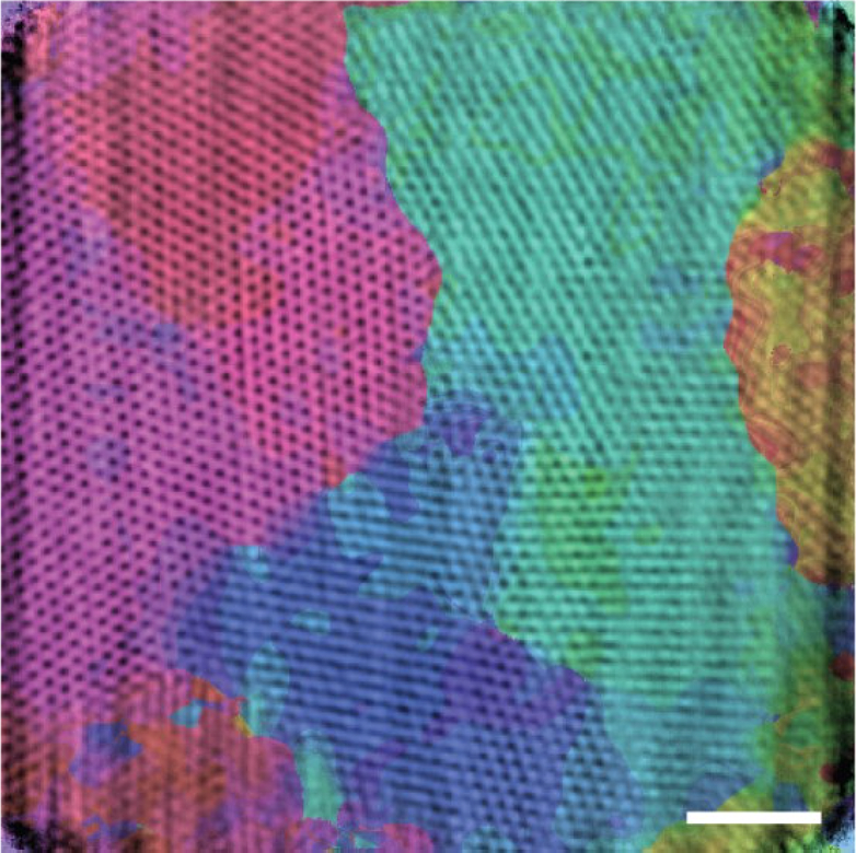
At sizes far too small to be seen by the human eye, the scales look like a flat patchwork map with sections of lattices, or “domains,” that are highly organized but have slightly different orientations.
“This explains why the scales appear to have a single color,” said UC San Diego’s Andrej Singer, who led the work. “We also found tiny crystal irregularities that may enhance light-scattering properties, making the butterfly wings appear brighter.”
These occasional irregularities appear as defects where the edges of the domains met each other.
“We think this may indicate the defects grow as a result of the chirality—the left or right-handedness—of the chitin molecules from which butterfly wings are formed,” said coauthor Ian McNulty, an x-ray physicist with the Center for Nanoscale Materials at Argonne, also a DOE Office of Science User Facility.
These crystal defects had never been seen before, he said.
Defects sound as though they’re a problem, but they can be very useful for determining how a material behaves—helping it to scatter more green light, for example, or to concentrate light energy in other useful ways.
“It would be interesting to find out whether this is an intentional result of the biological template for these things, and whether we can engineer something similar,” he said.
The observations, including that there are two distinct kinds of boundaries between domains, could shed more light on how these structures assemble themselves and how we could mimic such growth to give our own materials new properties, the authors said.
The x-ray studies provided a unique look because they are non-destructive—other microscopy techniques often require slicing the sample into paper-thin layers and staining it with dyes for contrast, McNulty said.
“We were able to map the entire three-micron thickness of the scale intact,” McNulty said. (Three microns is about the width of a strand of spider silk.)
See: Andrej Singer1*, Leandra Boucheron1, Sebastian H. Dietze1, Katharine E. Jensen2, David Vine3, Ian McNulty3, Eric R. Dufresne2, Richard O. Prum2, Simon G.J. Mochrie2, and Oleg G. Shpyrko1, "Domain morphology, boundaries, and topological defects in biophotonic gyroid nanostructures of butterfly wing scales," Sci. Advances 2 (6), e1600149-1 (2016). DOI: 10.1126/sciadv.1600149
Author affiliations: 1University of California, San Diego, 2Yale University, 3Argonne National Laboratory
Correspondence: * [email protected]
This work at the University of California, San Diego, was supported by the U.S. Department of Energy (DOE), Office of Science-Basic Energy Sciences (BES), under contract DE-SC0001805. S.G.J.M. was supported by the DOE BES under contract DE-SC0004162. Work at the Center for Nanoscale Materials and at the Advanced Photon Source was supported by the DOE Office of Science BES under contract DE-AC02-06CH11357.
Argonne National Laboratory seeks solutions to pressing national problems in science and technology. The nation's first national laboratory, Argonne conducts leading-edge basic and applied scientific research in virtually every scientific discipline. Argonne researchers work closely with researchers from hundreds of companies, universities, and federal, state and municipal agencies to help them solve their specific problems, advance America's scientific leadership and prepare the nation for a better future. With employees from more than 60 nations, Argonne is managed by UChicago Argonne, LLC for the U.S. Department of Energy's Office of Science.
The U.S. Department of Energy's Office of Science is the single largest supporter of basic research in the physical sciences in the United States and is working to address some of the most pressing challenges of our time. For more information, visit the Office of Science website.

