Multiferroics are materials that exhibit a ferroelectric and magnetic order simultaneously. These orders have been the building blocks for technologically and economically important applications such as ferroelectric memory and spintronics. The ferroelectric polarization couples strongly to ultraviolet light by exciting electron-hole pairs. The charge separation under the influence of remnant polarization generates a large electric field across the multiferroic film. These novel properties arising from light-matter interaction open opportunities for efficient electric-field control of magnetism on ultrafast time scales. To facilitate the application of multiferroics in new technologies, a microscopic picture needs to be developed to illustrate the process that starts from light-matter interaction and carries through to the relaxation of the photoinduced effects so that we can fully understand how these new properties come about and how best to harness them.
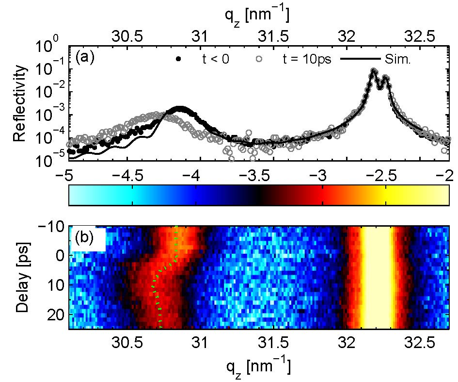
Recently, an international team led by scientists from the Universität Potsdam (Germany) in collaboration with colleagues from Fritz-Haber-Institute ( Germany), Helmholtz-Zentrum Berlin (Germany), Argonne National Laboratory, the University of Wisconsin-Madison, Cornell University, Stanford University, and Kavli Institute at Cornell for Nanoscale Science discovered a strong and inhomogeneous lattice deformation in a few-nanometer-thick film of BiFeO3after photoexcitation due to the generation of localized excited charge carriers.
Optical pump x-ray probe experiments were carried out at the Plasma X-ray Source (PXS) at the University of Potsdam (Germany) and at the X-ray Science Division 7-ID-C time-resolved beamline of the U.S. Department of Energy Office of Science’s Advanced Photon Source at Argonne. The combined analysis of the transient diffraction data from both the PXS and the APS allowed the researchers to follow the amplitude and spatial profile of photoinduced structural dynamics in BiFeO3on multiple time scales, from femtosecond up to microsecond delays under comparable excitation conditions. As a result, a new model of the dynamics and lattice coupling of photoexcited charge carriers in BiFeO3was developed and published in Physical Review Letters.
The researchers showed that the force driving the ultrafast lattice expansion in BiFeO3must be quasi-instantaneous (< 100-fs rise time), possibly due to the inverse piezoelectric effect caused by photoexcited charge carriers. Further, a strongly inhomogeneous deformation of the BiFeO3film from the picosecond up to the microsecond indicates a fast trapping and localization of these charge carriers.
The complete analysis of the diffraction data gives very detailed information on the material’s excitation and decay dynamics over several orders of time scales. This technique can be applied for a broad range of functional materials with a strong coupling of electronic degrees of freedom to the crystal lattice. The deeper understanding of the transient processes will allow for much faster and even more efficient devices in future technology.
Argonne physicist Haidan Wen, who helped to initiate the collaboration with the Dr. Bargheer group from the Universität Potsdam, said, “The success of this project exemplifies the synergetic collaboration of time-resolved research utilizing unique capabilities around the world to gain significant insight on the challenging problems that cannot be solved with the limited resources of any one institute.”
See: Daniel Schick1, Marc Herzog1,2, Haidan Wen3, Pice Chen4, Carolina Adamo5,6, Peter Gaal7, Darrell G. Schlom5,8, Paul G. Evans4, Yuelin Li3, and Matias Bargheer1,7*, “Localized Excited Charge Carriers Generate Ultrafast Inhomogeneous Strain in the Multiferroic BiFeO3,” Phys. Rev. Lett. 112, 097602 (2014). DOI:10.1103/PhysRevLett.112.097602
Author affiliations: 1Universität Potsdam, 2Fritz-Haber-Institut der Max-Planck-Gesellschaft, 3Argonne National Laboratory, 4University of Wisconsin-Madison, 5Cornell University, 6Stanford University, 7Helmholtz-Zentrum Berlin, 8Kavli Institute at Cornell for Nanoscale Science
Correspondence: * [email protected]
The work at Argonne was supported by the U.S. Department of Energy Office of Science-Basic Energy Sciences under Contract No. DE-AC02-06CH11357. Use of the Advanced Photon Source was supported by the U.S. Department of Energy, Basic Energy Sciences, Office of Science, under Contract No. DE-AC02-06CH11357.
The Advanced Photon Source at Argonne National Laboratory is one of five national synchrotron radiation light sources supported by the U.S. Department of Energy's Office of Science to carry out applied and basic research to understand, predict, and ultimately control matter and energy at the electronic, atomic, and molecular levels, provide the foundations for new energy technologies, and support DOE missions in energy, environment, and national security. To learn more about the Office of Science x-ray user facilities, visit http://science.energy.gov/user-facilities/basic-energy-sciences/.
Argonne National Laboratory seeks solutions to pressing national problems in science and technology. The nation's first national laboratory, Argonne conducts leading-edge basic and applied scientific research in virtually every scientific discipline. Argonne researchers work closely with researchers from hundreds of companies, universities, and federal, state and municipal agencies to help them solve their specific problems, advance America's scientific leadership and prepare the nation for a better future. With employees from more than 60 nations, Argonne is managed by UChicago Argonne, LLC for the U.S. Department of Energy's Office of Science.

