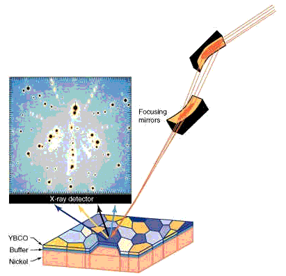
Materials ranging from massive steel girders to the microscopic aluminum wires in computer chips are made of grains - tiny crystals with diameters measured in millionths of a meter (microns). If scientists could "see" these individual grains, they could determine their orientation, as well as the effects of stress and chemical activity on them. They might also be able to determine how best to jam more circuits together in microelectronic components, making them smaller and faster, so computers could perform complex functions - such as speech recognition - more quickly. They could also find out to what extent grains of a superconducting material mimic the alignment of the substrate on which the material is grown; discovery of such orientation replication involving deposited thin films is essential to the design of effective high-temperature superconductors.
Scientists are now able to study the fine details of grain behavior in materials, thanks to new x-ray beamlines at the Advanced Photon Source (APS), an intense synchrotron x-ray source at DOE's Argonne National Laboratory. Oak Ridge National Laboratory (ORNL) is a leader in efforts to develop microbeams at the APS. Microbeams are x-rays that are focused down to beam diameters smaller than one micron, allowing researchers to see a material's microstructural features within individual grains. The instrumented beamlines now enable researchers to perform micro-diffraction x-ray scattering using beams of submicron dimensions. These microbeams will provide access for the first time to the mesoscale, the length scale that determines the macroscopic properties of many materials.
ORNL scientists have also performed experiments using microbeam analysis with a resolution of <1 µm. They are studying strain in integrated circuit wires, a major source of electrical problems in developing smaller, denser microelectronic components for the next generation of computers. They are also investigating the epitaxy of oxide films on nickel foils and the defects introduced by ion-implantation processing in silicon to help in understanding and improving materials properties.
The initial design, microbeam optics, and associated techniques for materials analysis are being developed by ORNL and Howard University at the APS on the MHATT-CAT beamline constructed by the University of Michigan, Howard University (a historically black university), and Lucent Technologies Collaborative Access Team. To exploit microbeam capabilities fully, ORNL is developing a dedicated microbeam facility directed toward 0.1 µm resolution on the recently commissioned UNI-CAT synchrotron beamline. (UNI-CAT stands for University National Laboratory Industry Collaborative Access Team.) UNI-CAT is a $10-million collaboration involving ORNL, the University of Illinois, the National Institute of Standards and Technology, and UOP Research, Inc. UNI-CAT provides access to the nation's most intense x-ray beams for a wide range of studies of the structure and properties of materials. ORNL has received funding through the new-initiative competition of the Division of Materials Science in DOE's Office of Basic Energy Sciences to develop a mesoscale-materials program at the APS using microbeams.
From "Facilitating Science: ORNL Research at User Facilities" Oak Ridge National Laboratory Review Volume 32, Number 2, 1999.
The full text of this article is available at: http://www.ornl.gov/ORNLReview/v32_2_99/fac.htm

