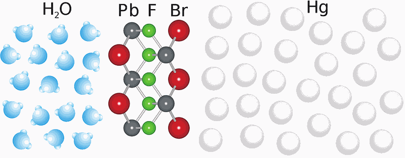
Liquid interface behavior cannot be investigated at atomic level by most modern methods. Only brilliant X-rays at world-leading light sources can investigate this type of important chemical processes.
The result is reported on in the April issue of the journal Proceedings of the National Academy of Science in an article titled “In situ x-ray studies of adlayer-induced crystal nucleation at the liquid-liquid interface.”
The team used high-energy, high-brilliance X-rays at the LSS (liquid surface spectrometer) at the 9-ID-C beamline of the U.S. Department of Energy Office of Science’s Advanced Photon Source at Argonne National Laboratory and the LISA diffractometer (Liquid Interfaces Scattering Apparatus) at the PETRA III light source at the German laboratory DESY. The research is the continuation and expansion of research done at the APS in 2010.
In their latest work, the researchers from the U.S., Israel and Germany wanted to find out, for the first time, what exactly occurs during chemical growth at liquid interfaces. Led by researchers from the Institute of Experimental and Applied Physics of Kiel University, the team observed the formation of an ordered crystal of exactly five atomic layers between the two liquids, which acts as a foundation for growing even bigger crystals. This work may result in new semiconductor and nanoparticle production processes.
They investigated mercury surface in contact with a salt solution containing lead and bromine (or fluorine) ions and obtained an astonishing result: although both liquids were atomically disordered in the bulk, a nanometer-thin layer that is a ten thousandth of the width of a human hair, with crystalline order was formed at their interface.
The atomic order that develops at the interface of otherwise disordered liquids is not only of fundamental interest for science. In fact, in the last few years, a range of chemical processes for producing materials and nano-particles has employed growth at liquid interfaces. For example, two years ago, American scientists at the University of Michigan developed a similar process for manufacturing semiconductor germanium with an extremely energy-efficient method from its oxide.
Further developments of such processes could help to reduce the high energy costs in the production of solar cells. In order to make such advances, a better understanding of these processes on the atomic scale is required. This work is an important step in this direction.
The original Argonne National Laboratory feature story by Tona Kunz can be read here.
The Advanced Photon Source at Argonne National Laboratory is one of five national synchrotron radiation light sources supported by the U.S. Department of Energy’s Office of Science to carry out applied and basic research to understand, predict, and ultimately control matter and energy at the electronic, atomic, and molecular levels, provide the foundations for new energy technologies, and support DOE missions in energy, environment, and national security. To learn more about the Office of Science x-ray user facilities, visit http://science.energy.gov/user-facilities/basic-energy-sciences/.
Argonne National Laboratory seeks solutions to pressing national problems in science and technology. The nation's first national laboratory, Argonne conducts leading-edge basic and applied scientific research in virtually every scientific discipline. Argonne researchers work closely with researchers from hundreds of companies, universities, and federal, state and municipal agencies to help them solve their specific problems, advance America's scientific leadership and prepare the nation for a better future. With employees from more than 60 nations, Argonne is managed by UChicago Argonne, LLC for the U.S. Department of Energy's Office of Science.

